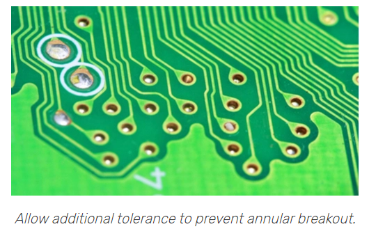
← FX5 16EX ES Wiring Diagram: The Industrial Automation Secret Fx5-16ex/es: limited time exclusive from ribhu international Wiring Diagram Sony Drive: The CDX Car Stereo Installation Secret Electrical wiring components electrical wiring diagram, elec →
If you are looking for The Ultimate Guide to Understanding Via Plating Thickness in PCBs - Top you've came to the right page. We have 25 Images about The Ultimate Guide to Understanding Via Plating Thickness in PCBs - Top like Detailed Procedures of Plating Copper for PCB Processing - PCB, Detailed Procedures of Plating Copper for PCB Processing - PCB and also Detailed Procedures of Plating Copper for PCB Processing - PCB. Here it is:
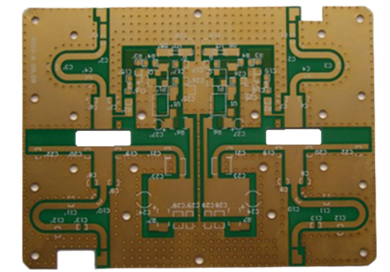
The Ultimate Guide To Understanding Via Plating Thickness In PCBs - Top
 camtechpcb.com
The Ultimate Guide to Understanding Via Plating Thickness in PCBs - Top ...
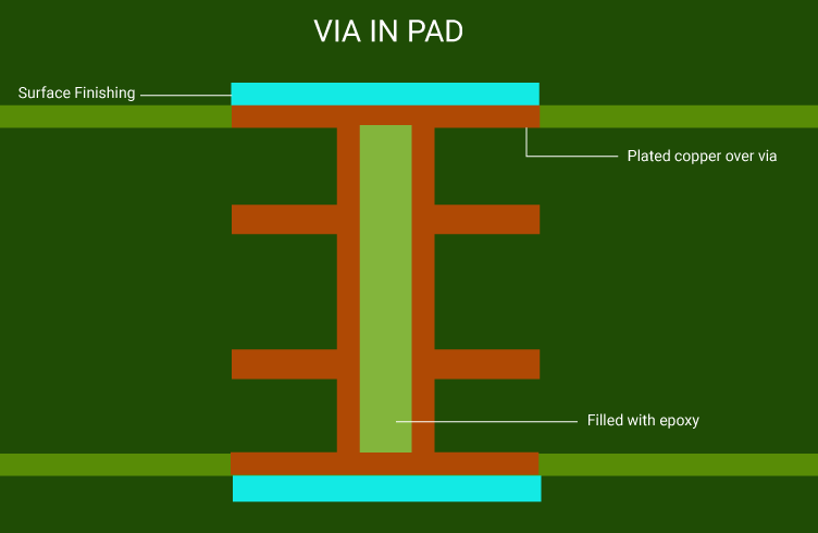
Via-in-Pad In PCB Design Manufacturing | Sierra Circuits
 www.protoexpress.com
Via-in-Pad in PCB Design Manufacturing | Sierra Circuits
Inspirasi Pcbway Via Plating Thickness, Skema Pcb
 skemadriver.blogspot.com
Inspirasi Pcbway Via Plating Thickness, Skema Pcb
The Ultimate Guide To Understanding Via Plating Thickness In PCBs - Top
 camtechpcb.com
The Ultimate Guide to Understanding Via Plating Thickness in PCBs - Top ...
The Ultimate Guide To Understanding Via Plating Thickness In PCBs - Top
 camtechpcb.com
The Ultimate Guide to Understanding Via Plating Thickness in PCBs - Top ...
PCB & PCB Assembly Reviews - Share - PCBWay
 www.pcbway.com
PCB & PCB Assembly Reviews - share - PCBWay
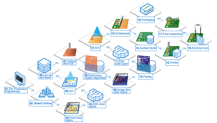
PCB Manufacturing Process & Equipment - PCBWay
 www.pcbway.com
PCB manufacturing Process & Equipment - PCBWay
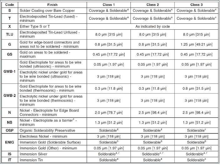
IPC Standards For Surface Plating
 www.sharedpcb.com
IPC Standards for Surface Plating
Inspirasi Pcbway Via Plating Thickness, Skema Pcb
 skemadriver.blogspot.com
Inspirasi Pcbway Via Plating Thickness, Skema Pcb
Explaining Via-filling Plating In PCB Manufacturing Process - RayPCB
 www.raypcb.com
Explaining Via-filling Plating in PCB Manufacturing Process - RayPCB
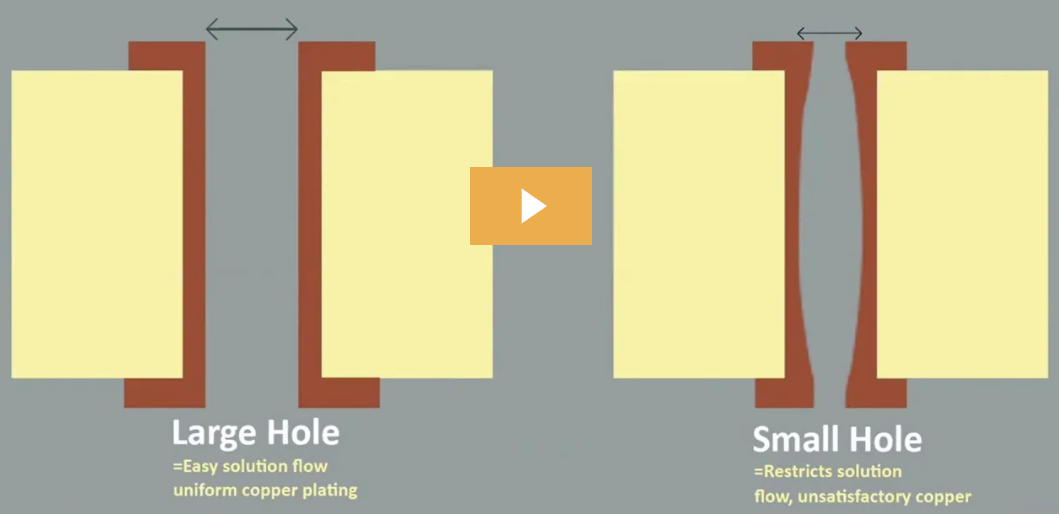
PCB Via Plating: Depth Guide And Process - Jhdpcb
 jhdpcb.com
PCB Via Plating: Depth Guide And Process - Jhdpcb
Inspirasi Pcbway Via Plating Thickness, Skema Pcb
 skemadriver.blogspot.com
Inspirasi Pcbway Via Plating Thickness, Skema Pcb
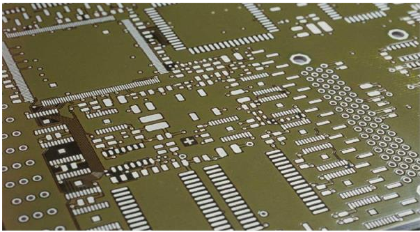
Detailed Procedures Of Plating Copper For PCB Processing - PCB
 www.pcbway.com
Detailed Procedures of Plating Copper for PCB Processing - PCB ...
The Ultimate Guide To Understanding Via Plating Thickness In PCBs - Top
 camtechpcb.com
The Ultimate Guide to Understanding Via Plating Thickness in PCBs - Top ...
Inspirasi Pcbway Via Plating Thickness, Skema Pcb
 skemadriver.blogspot.com
Inspirasi Pcbway Via Plating Thickness, Skema Pcb
The Ultimate Guide To Understanding Via Plating Thickness In PCBs - Top
 camtechpcb.com
The Ultimate Guide to Understanding Via Plating Thickness in PCBs - Top ...
Copper Wrap Plating For PCB Manufacturing | Sierra Circuits
 www.protoexpress.com
Copper Wrap Plating for PCB Manufacturing | Sierra Circuits
Inspirasi Pcbway Via Plating Thickness Skema Pcb - Vrogue.co
 www.vrogue.co
Inspirasi Pcbway Via Plating Thickness Skema Pcb - vrogue.co
Standard PCB Thickness - Determine The Right Standards
 www.ourpcb.com
Standard PCB Thickness - Determine the Right Standards
The Ultimate Guide To Understanding Via Plating Thickness In PCBs - Top
 camtechpcb.com
The Ultimate Guide to Understanding Via Plating Thickness in PCBs - Top ...
Why Some PCBs Need Edge Plating? - Technology - PCBway
 www.pcbway.com
Why Some PCBs Need Edge Plating? - Technology - PCBway
The Ultimate Guide To Understanding Via Plating Thickness In PCBs - Top
 camtechpcb.com
The Ultimate Guide to Understanding Via Plating Thickness in PCBs - Top ...
The Ultimate Guide To Understanding Via Plating Thickness In PCBs - Top
 camtechpcb.com
The Ultimate Guide to Understanding Via Plating Thickness in PCBs - Top ...
Detailed Procedures Of Plating Copper For PCB Processing - PCB
 www.pcbway.com
Detailed Procedures of Plating Copper for PCB Processing - PCB ...
PCB Edge Plating - A Complete Guide - IBE Electronics
 www.pcbaaa.com
PCB edge plating - a complete guide - IBE Electronics
Why some pcbs need edge plating?. The ultimate guide to understanding via plating thickness in pcbs. Inspirasi pcbway via plating thickness, skema pcb